We may not have the course you’re looking for. If you enquire or give us a call on +44 1344 203 999 and speak to our training experts, we may still be able to help with your training requirements.
Training Outcomes Within Your Budget!
We ensure quality, budget-alignment, and timely delivery by our expert instructors.
The question "What is a Transistor?" delves into is the very cornerstone in modern electronic systems. The ability of a Transistor to allow the binary data code, whether in a form of 0s and 1s, ultimately underlies whatever form of communication or computation in the digital domain.With Statista quoting manufacturer sales of Transistors to have reached £212.4 million in the UK in 2021, the question of What is a Transistor became the more pressing question. This rise from the previous year further cemented a rising trend for Transistors in the purchase of electronic components. In this blog, we will understand the Transistor and its types in more detail.
Table of Contents
1) What is a Transistor?
2) Types of Transistors
3) How does a Transistor work?
4) History of Transistors
5) Pros and Cons of the Transistors
6) Conclusion
What is a Transistor?
"Transistor" means a special class of semiconductor device in which the electric signals, like current or voltage, are regulated or controlled. It was made and demonstrated on December 23, 1947, by the three scientists of America: John Bardeen, Walter Brattain, and William Shockley. Then, a small-resistance circuit usually takes a feeble signal into a big-resistance circuit using a switching device or a small gadget.
The transistors form logic gates when placed along with different configurations, which can be combined into arrays (half adders) or full adders. The Transistor consists of two PN diodes that are connected back-to-back. It also contains three terminals for input, output, and control switching functions. These three terminals of the transistors are named a base, an emitter, and a collector.
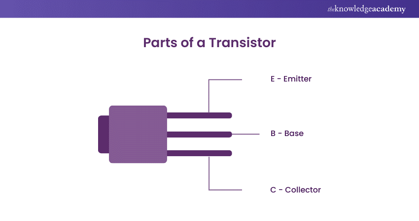
These terminal names are provided based on the transistor's common terminal. It is frequently encountered as discrete pieces in circuit boards or implemented into integrated circuits. It is a crucial building block for contemporary technological gadgets.
During doping, a chemical procedure used to make Transistors, the semiconductive material gains an additional positive charge (P-type) or a negative charge (N-type). It may be done in a PNP or NPN design, with the intermediate material as the base or flow control. When the voltage or current in the middle base layer changes slightly, electricity flows across the entire component, which can be used as an amplifier.

History of Transistors
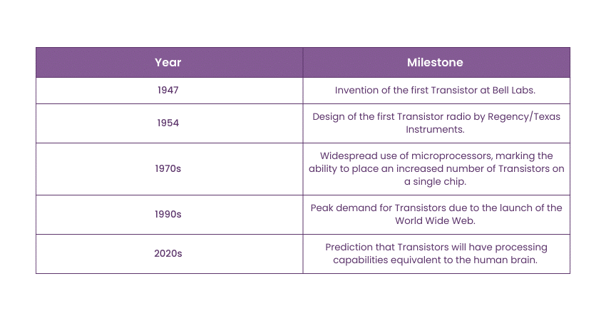
The following image shows the development of Transistors since the invention of the first Transistor.
Types of Transistors
Transistors are mainly divided into two types based on the use of circuits.
Bipolar Junction Transistor (BJT)
The Bipolar Junction Transistor has three terminals:
a) the base
b) the emitter
c) the collector
As such, even a very small current that passes into the base region of the Transistor can hence be made to control a much larger current flow between the collector and emitter terminal. Two basic types are:
a) PNP Transistors
b) NPN Transistors
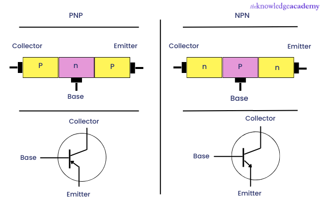
PNP Transistor: This Transistor is made of two p-type semiconductor materials; in between, it holds an n-type semiconductor material. A thin layer of n-type semiconductor is used between these two p-type materials. The PNP Transistor is comprised of two series-connected crystal diodes. Additionally, in this configuration, the device also regulates the current flow. These Transistors diodes are divided into two sides: a collector-base diode on the right and an emitter-base diode on the left.
In PNP Transistors, holes make up most charge carriers, while electrons are the minority charge carriers. The arrow sign in this Transistor indicates the regular current flow, which flows from the emitter terminal and exits at the collector terminal. The PNP Transistor is shown with a symbol in the image provided below.
NPN Transistor: The NPN Transistor has two n-type materials and a thin layer of p-type semiconductor introduced in the middle. The primary job of the NPN Transistor is to transform weak signals into strong signals. When electrons transfer from the emitter to the collector area of an NPN Transistor, current flows through the Transistors. Since NPN Transistors' electron mobility is higher than holes' mobility, they are currently utilised often. The NPN Transistor with a symbol is displayed in the image below.
Field Effect Transistor
Field Effect Transistors (FET) comprise the Gate, Source, and Drain terminals. These types of transistors are regarded as voltage-controlled components. The Gate terminal manages the current between the Source and the Drain. This transistor conducts electricity using either a P-channel Field Effect Transistor or an N-channel Field Effect Transistor. The Field Effect Transistor can be seen in the figure below.
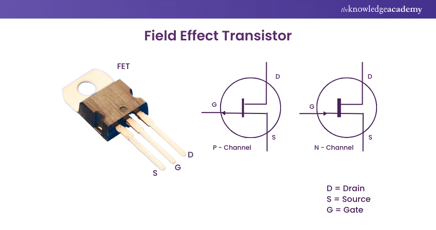
According to Ohm's law, the current is inversely related to the impedance of the circuit. If the impedance is high, the current will be very low. Field Effect Transistors, therefore, draw extremely minimal current from the power supply of a circuit.
Hence, the power elements attached to transistors do not interfere with the transistors as a result. Field Effect Transistors lack the significant amplification that bipolar transistors produce, which is the fundamental drawback of FETs.
The benefits provided by Field Effect Transistors include simpler manufacturing, low cost, and less loading. However, bipolar transistors are superior because they offer better amplification.
The two primary types of Field Effect Transistors are Junction Field Effect Transistors (JFETs) and Metal Oxide Silicon Field Effect Transistors (MOSFETs). Compared to Junction Field Effect Transistors (JFETs), the input impedance values of (MOSFETs) are more significant.
Are you interested in pursuing your Internet of Things (IoT) career? Then, join the Internet Of Things IoT Systems And Applications Training course now!
How does a Transistor work?
Since silicon has a higher current capacity, a higher voltage rating, and is less sensitive to temperature, it is usually used to make Transistors. The emitter-base segment is kept forward-biased and travels through the base area to establish the base current. The magnitude of the base current is very minute. For the electrons to move from the base area into the collector region, a hole must be created by the base current.
Transistors have fewer electrons than emitters because the transistor base is very narrow and mildly doped. These few electrons from the emitter move to the collecting area. Therefore, collector current can be obtained by altering the base area.
The base-emitter junction and the base-collector junction of a Bipolar Junction Transistor (BJT) are typically forward and reverse-biased.
Let's use an NPN transistor as an example to demonstrate how a Transistor functions. The current carriers in a PNP transistor are holes, and the voltages are reversed. The other applied concepts are the same as those in a PNP transistor.
NPN Transistor Operations
As the emitter of the NPN device is fabricated from n-type material, most carriers in this section shall be electrons. When the junction between base and emitter is forward-biased, holes of the minority carrier will move in the n-type region, and electrons will move from the n-type region to the p-type region.
When they come into contact, the holes and electrons merge, allowing current to flow across the junction. When the junction is reverse-biased, the holes and electrons leave, causing a depletion region to develop between the two regions where no current can pass.
When a current passes between the base and the emitter, electrons leave the emitter and flow into the base. When the electrons enter the depletion area, they often unite.
However, this location has very little doping and a very thin foundation. This indicates that most electrons may travel the area without recombining with holes. Therefore, the electrons will move in the direction of the collector, so the current will flow in the collector circuit.
How do Transistors work in calculators and computers?
Transistors are the building blocks of calculators and computers, acting as tiny switches that can turn on and off, representing the binary states of 0 and 1. In calculators, Transistors form logic gates like AND, OR, and NOT, which perform calculations by processing binary inputs into outputs1.
In computers, millions of Transistors switch between these binary states to execute complex tasks and calculations. This binary language of Transistors is what enables devices to process and store information, making them integral to the functionality of modern electronics.
Pros and Cons of the Transistors
Let us discuss the advantages and disadvantages of the Transistors in the following table.
|
Pros |
Cons |
|
1) Has a longer shelf life. 2) It is a tiny size, and the costs are not high too. 3) For the Bipolar Junction Transistors, the output impedance is the lowest, and the input impedance is the highest. 4) Voltage consumption is very low. 5) Can bear mechanical vibrations. 6) The cathode heater in the transistor does not consume power. |
1) Difficult to trace the failure point due to its tiny size. 2) Also, unsoldering the old transistors to replace them with new ones is difficult. 3) Complex manufacturing techniques are used to build a transistor. 4) It can get damaged during a second breakdown. 5) Low reverse blocking capacity. |
Master Computer Troubleshooting with our Computer Hardware Troubleshooting Course and boost your IT skills today!
Conclusion
In this blog, we have understood What is a Transistors; Transistors are in huge demand and serve various purposes in electronic devices. They are used widely in complex switching circuits in almost every kind of latest telecommunication system.
Are you interested in understanding AutoCAD Electrical software? Then join the AutoCAD Electrical Training course now!
Frequently Asked Questions

Critical evolutions for electronics, thanks to Transistors, have made devices much smaller in size yet improved their performance and reduced the consumption of power. Among other most recent developments, we have 3D-stacked CMOS, which has boosted Moore’s Law.

The three-terminal Transistor structure—emitter, base, and collector—can thus provide a controlled pathway for the flow of electrons. The amplification results in a small current, which is introduced at the base terminal, which can control a large current between the collector and emitter.

The Knowledge Academy takes global learning to new heights, offering over 30,000 online courses across 490+ locations in 220 countries. This expansive reach ensures accessibility and convenience for learners worldwide.
Alongside our diverse Online Course Catalogue, encompassing 17 major categories, we go the extra mile by providing a plethora of free educational Online Resources like News updates, Blogs, videos, webinars, and interview questions. Tailoring learning experiences further, professionals can maximise value with customisable Course Bundles of TKA.

The Knowledge Academy’s Knowledge Pass, a prepaid voucher, adds another layer of flexibility, allowing course bookings over a 12-month period. Join us on a journey where education knows no bounds.

The Knowledge Academy offers various IT Support and Solution Courses, including Networking Training and Computer Hardware Troubleshooting Courses. These courses cater to different skill levels, providing comprehensive insights into Computer Network.
Our IT Infrastructure & Networking Blogs cover a range of topics related to IT Solutions, offering valuable resources, best practices, and industry insights. Whether you are a beginner or looking to advance your IT Solutions skills, The Knowledge Academy's diverse courses and informative blogs have you covered.
Upcoming Office Applications Resources Batches & Dates
Date
 AutoCAD Electrical Training
Fri 28th Feb 2025
Fri 4th Apr 2025
Fri 27th Jun 2025
Fri 29th Aug 2025
Fri 24th Oct 2025


 Top Rated Course


 If you wish to make any changes to your course, please


